
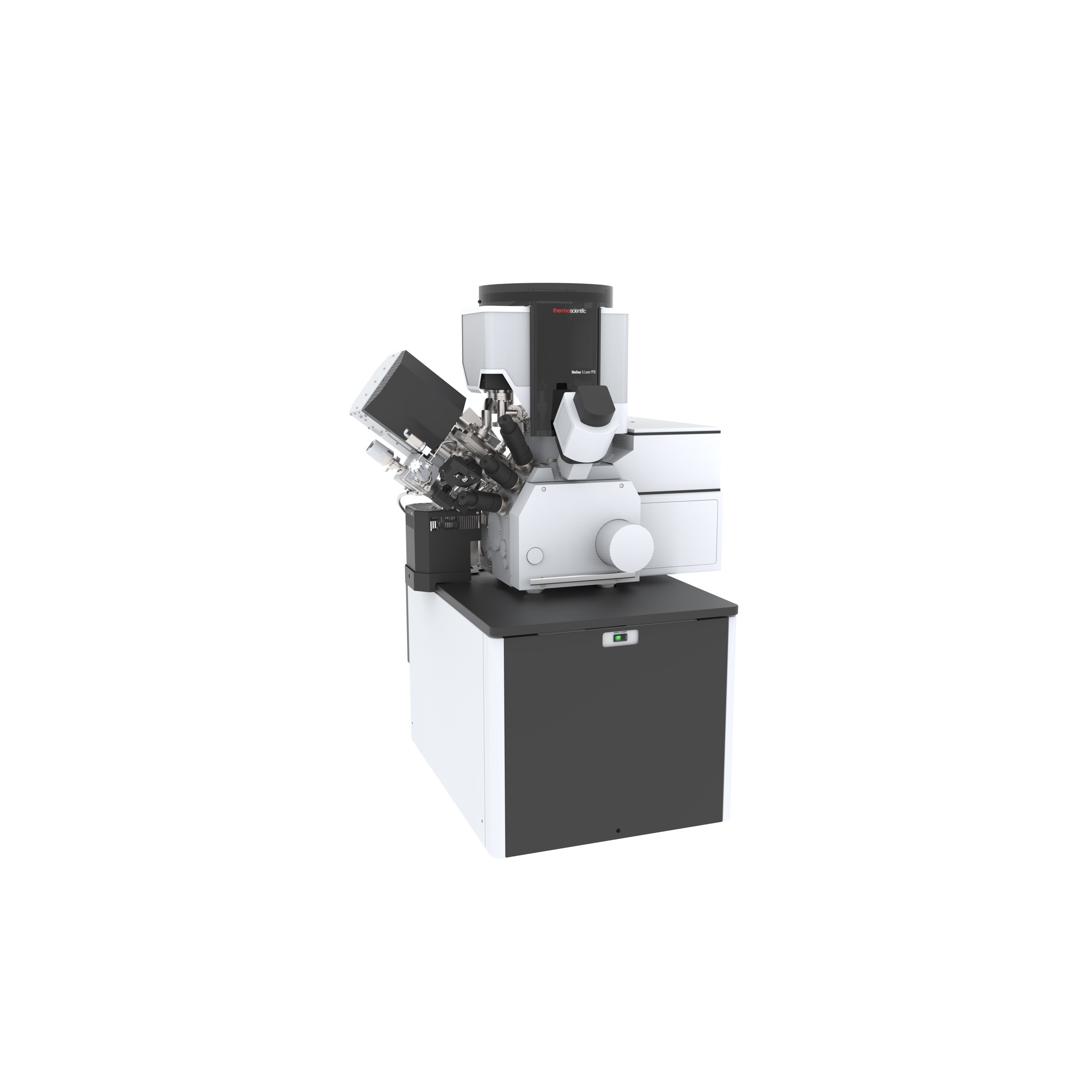
Thermo Fisher Scientific has developed a focused ion beam scanning electron microscope (FIB-SEM) with a femtosecond laser that it says can characterize millimeter-scale volumes of material in 3D with nanometer resolution. According to the company, the Helios 5 Laser plasma focused ion beam (PFIB) system can carry out high-resolution imaging and analytical capabilities with a FIB column while the femtosecond laser can enable in-situ ablation at material removal rates not previously obtained by a commercially available product.
The FIB-SEM can be used to analyze a variety of materials including metals, batteries, glass, ceramics, paint coatings, polymers, biomaterials and graphite. ‘The Helios 5 Laser PFIB dramatically accelerates the pace of research for both academic and industrial users, allowing them to characterize materials in a matter of minutes versus the days it took before,’ said Rosy Lee, vice president of materials science at Thermo Fisher. ‘Not only can researchers quickly and accurately image statistically relevant, site-specific, millimeter-size cross-sections at nanoscale resolution, they can also set up large-volume 3D analyses to be automatically completed overnight, freeing up the microscope for other uses.’ The Helios 5 Laser PFIB allows researchers to obtain accurate large-volume 3D and sub-surface data up to 15,000 times faster than a typical Gallium ion source focused ion beam (Ga-FIB), Thermo Fisher said, while for some materials, a large cross-section of hundreds of microns can be milled by the Helios 5 Laser PFIB in less than five minutes. Serial-section tomography is now possible with this combination of laser and llasma FIB, and when combined with energy-dispersive (EDS) and electron backscatter diffraction (EBSD) detectors, can be extended to 3D elemental and grain orientation analysis at the millimeter scale.
This story uses material from Thermo Fisher, with editorial changes made by Materials Today. The views expressed in this article do not necessarily represent those of Elsevier.

